
Suggestions on placing the MOSFETs to prevent ringing LT Spice circuit simulation for begginers
General guideliness
Based on the Eric Bogatin on Breaking Bad Habits in PCB Design.Some additional details in his article
Signal trace width - 6 mil (1 Amp max)
Power traces - 20 mil (3 Amp max)
Drilled diameter for signal traces - 13 mil - narrow via to get higher interconnectency
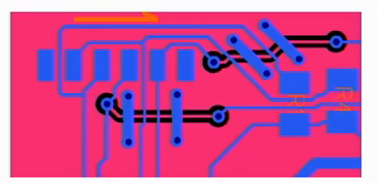
If one must route something on bottom layer, make path short and use bridges (return strap) as on the picture:
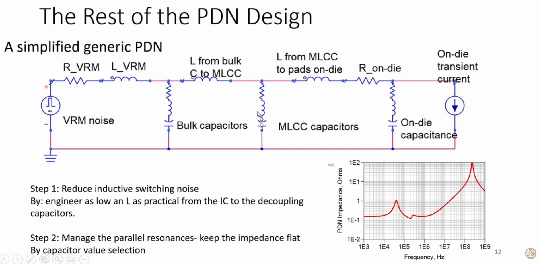

- Smaller value would have lower inductance (to lower down impedance on higher frequences)
- Larger values will provide needed capacitance for the device
Some useful guideliness from YouTube
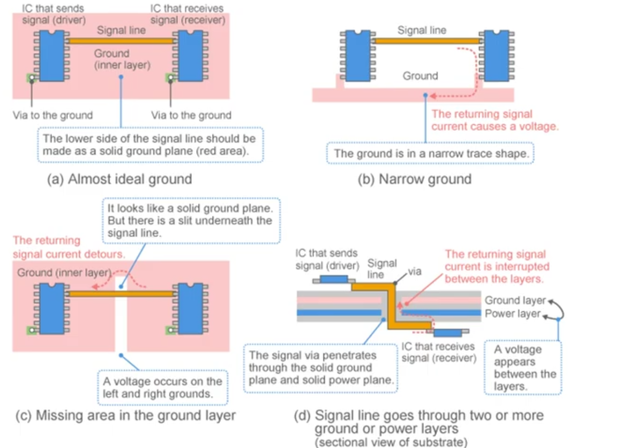
Careful about the return paths:
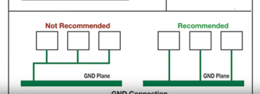
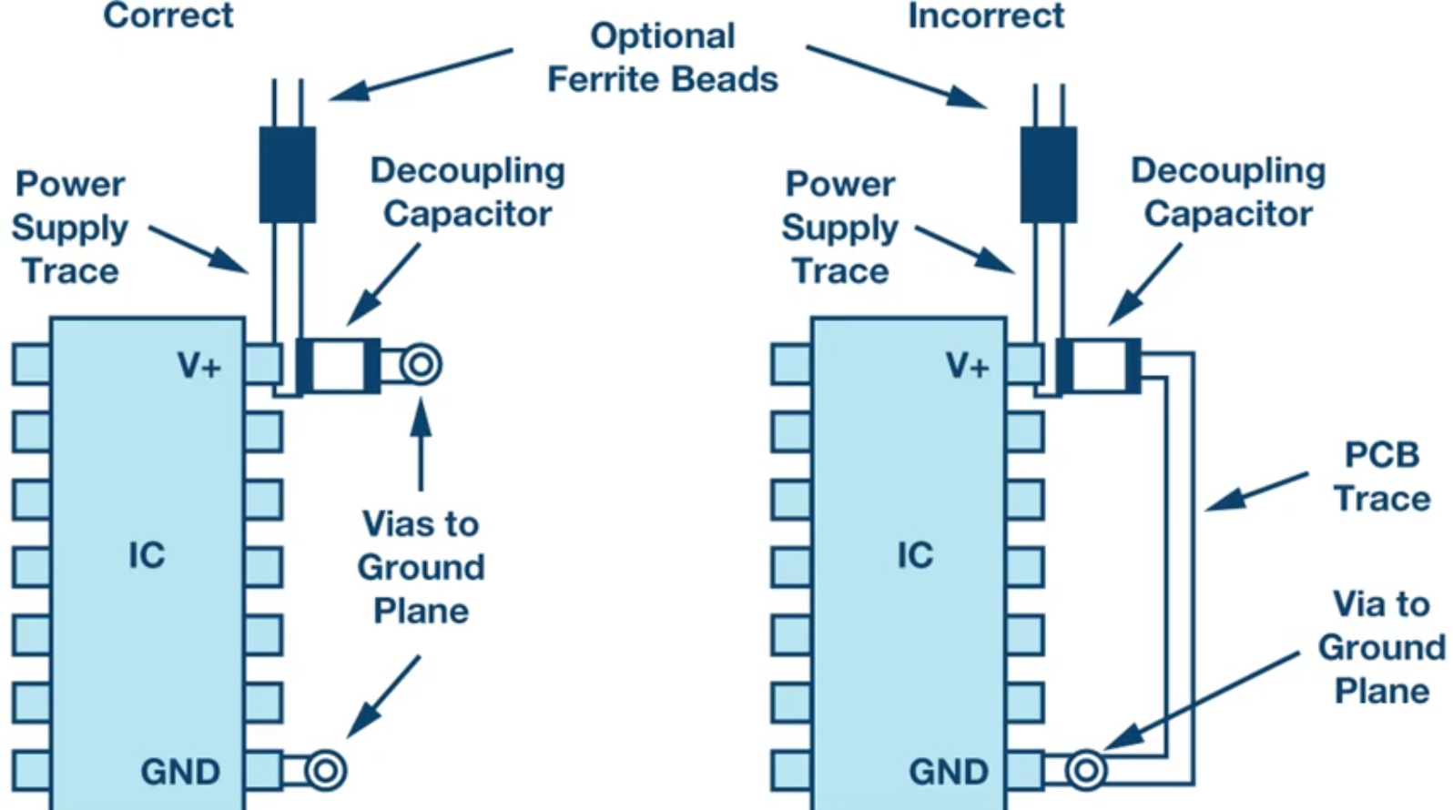
Suggestion on ground connection:
Watch out traces:
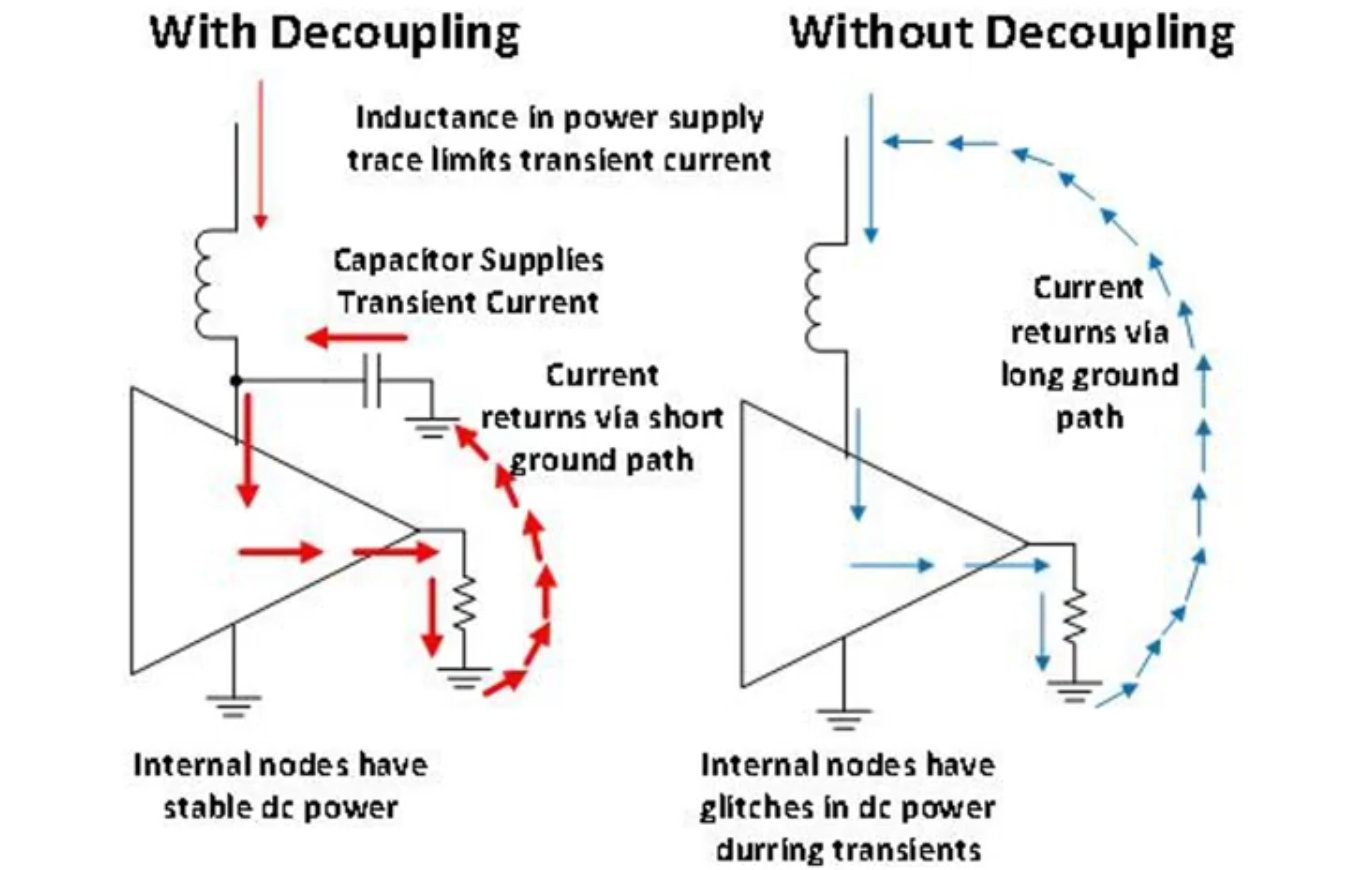
Paths when decopling introduced:
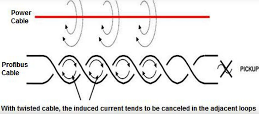
Reason behind twisting the power cables:
Thermal via size is important- if too large, termal vias will wick the solder material which can result in poor connection of the termal pad to the package. Based on Texas instruments application note it is suggested to use 0.33mm drill size via, or smaller (with copper plated barrell for conductivity)